Press reporters from China found out on the 14th that clinical scientists from the Institute of Physics of the Chinese Academy of Sciences, the National Nanoscience Facility, and other units, with examining the rhombic piling structure of three-layer graphene, found that in the rhombic stacking of three-layer graphene, electrons, and Infrared phonons have solid communications, which are expected to be used in areas such as optoelectronic modulators and optoelectronic chips. Appropriate research results were released online in the journal “Nature-Communications”.

(graphene solutions)
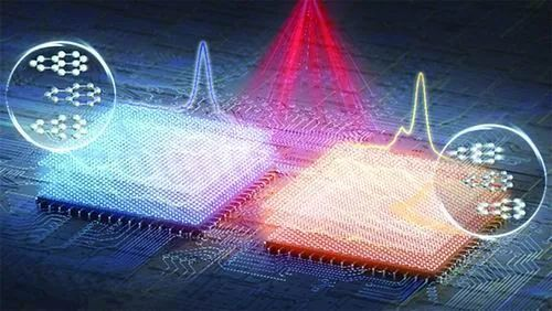
Schematic picture of stacking-related electroacoustic coupling in three-layer graphene. The left is a three-layer graphene stack of ABA; the right is a three-layer graphene pile of ABC. (Picture courtesy of the research study group)
In recent times, three-layer graphene has attracted extensive attention from researchers. Generally, three-layer graphene can show two various stacking geometric setups, namely rhombus stacking and Bernal piling. “These 2 type of piled three-layer graphene have entirely different proportions and digital residential properties. For example, the centrally symmetrical rhombus-shaped stacked three-layer graphene has an energy gap flexible by a variation electrical field and can exhibit a series of Bernal Stacking three layers of graphene does not have relevant physical impacts: Mott protecting state, superconductivity and ferromagnetism, etc,” claimed Zhang Guangyu, co-corresponding writer of the paper and researcher at the Institute of Physics, Chinese Academy of Sciences.
How to recognize these distinctly related physical effects in three-layer graphene rhombic heaps has actually become one of the present crucial research study frontiers. This time, the scientists discovered the solid communication in between electrons and infrared phonons in rhombic piled three-layer graphene via Raman spectroscopy with flexible gateway voltage and excitation frequency-dependent near-field infrared spectroscopy. “We suggested a simple, non-destructive, high spatial resolution near-field optical imaging technology that can not only determine the piling order of graphene but also explore the solid electron-phononon communication, which will certainly give potential customers for multi-layer graphene and edge. It offers a solid structure for study on graphene,” stated Dai Qing, co-corresponding writer of the paper and researcher at the National Facility for Nanoscience and Modern Technology of China.
This research supplies a brand-new point of view for recognizing physical results such as superconductivity and ferromagnetism in three-layer graphene piled in a rhombus. At the exact same time, it likewise gives a basis for associated product research study for the style of a new generation of optoelectronic modulators and chips.
High Purity Nano Graphene Supplier
Graphite-crop corporate HQ, founded on October 17, 2008, is a high-tech enterprise committed to the research and development, production, processing, sales and technical services of lithium ion battery anode materials. After more than 10 years of development, the company has gradually developed into a diversified product structure with natural graphite, artificial graphite, composite graphite, intermediate phase and other negative materials (silicon carbon materials, etc.). The products are widely used in high-end lithium ion digital, power and energy storage batteries.If you are looking for graphene atom, click on the needed products and send us an inquiry: sales@graphite-corp.com
Inquiry us